Researchers in China have achieved continuous wave (cw) lasing at room temperature for indium gallium nitride (InGaN) laser diodes (LDs) grown directly on silicon (Si) [Yi Sun et al, Nature Photonics, 10, p595, 2016].
The team from Suzhou Institute of Nano-Tech and Nano-Bionics (SINANO), Huazhong University of Science and Technology, and Wuhan University, comments: "With further improvements in the material quality, device performance and life-time, GaN-on-Si technology holds great promise for commercializing III-nitride laser diodes on large-diameter and cost-effective substrates. Moreover, by growing GaN upon Si(111)-on-insulator-Si(100), InGaN-based LDs could be a useful alternative on-chip light source for monolithic-integrated Si photonics."
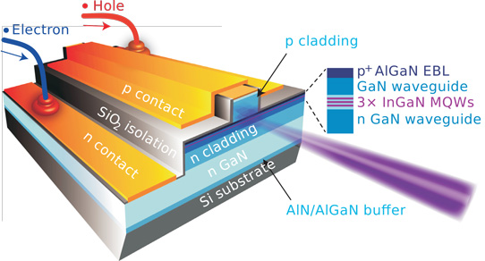
Figure 1. Schematic architecture of InGaN-based laser diode directly grown on silicon.
Presently, integrating silicon with laser diodes involves difficult bonding of separate chips on the silicon platform, which is not generally compatible with large-scale wafer-level manufacturing as required by foundries.
The epitaxial material was grown by metal-organic chemical vapor deposition (MOCVD). The researchers used a sequence of aluminium gallium nitride (AlGaN) and aluminium nitride buffer interlayers to manage the differences in lattice parameter (~17%) and coefficient of thermal expansion (CTE ~ 54%) between Si and GaN that lead to threading dislocations (TDs) and cracking. TDs act as non-radiative recombination centers, reducing efficiency and increasing heat dissipation leading to device degradation.
The team comments: "It is found that the compressive strain that accumulates via the AlN/Al0.35Ga0.65N/Al0.17Ga0.83N multi-layer buffer can not only compensate for the tensile stress due to the CTE mismatch during cool down, but also induce the inclination and annihilation of TDs at the interfaces, according to cross-sectional transmission electron microscopy (TEM) observations."
The researchers estimate that the TD density in the subsequent GaN layer was 5.8x10⁸/cm2, a value comparable to GaN grown on sapphire. After the addition of the laser diode layers to the GaN-on-Si template, the epitaxial film was 5.8μm thick and crack-free with wafer bow less than 10μm.
Table 1. Epitaxial structure.
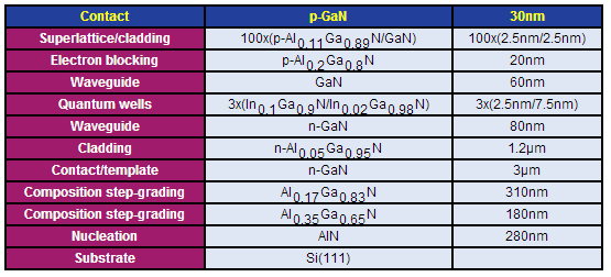
The epitaxial material (Table 1) was formed into lateral laser diodes (Figure 1) with 4μmx800μm ridges. The facets were cleaved and coated with reflective titanium dioxide and silicon dioxide quarter-wave layer pairs – 3 pairs on the front and 7 pairs on the back. The yield of laser-capable devices was 94%.
The laser diode was tested under pulsed and CW current injection at room temperature. In pulsed operation there was a blue shift from 415.9nm to 413.4nm with increasing current (50mA to 160mA). This is attributed to screening of the quantum-confined Stark effect. The full-width at half maximum (FWHM) was 0.64nm for stimulated emission.
For cw operation, stimulated emission began around 150mA (4.7kA/cm2 density). The cw operation lifetime at 180mA was about a minute before a dramatic decay of output power. The researchers attribute the short life to an imperfect p-n junction doping profile and to the high TD density, relative to devices produced 'homoepitaxially' on bulk or free-standing GaN substrates (TD density ~ 106/cm2).
The poor doping profile leads to a high forward voltage of 8.5V, giving joule heating. The researchers comment: "Previous reports showed that the lifetime of InGaN-based laser diode grown on a sapphire substrate was improved from a few seconds to 300h when the operation voltage was reduced from 8 to 4V."
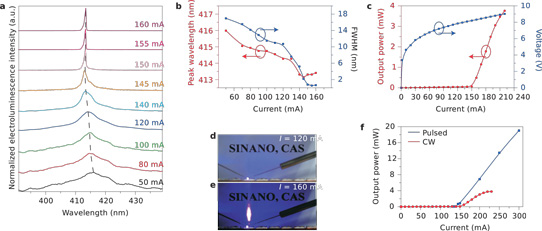
Figure 2. Characteristics: a, Electroluminescence spectra under various 1μs 10kHz pulsed currents at room temperature. b, Peak wavelength and full-width at half-maximum (FWHM) as a function of pulsed current at room temperature. c, Output power, current, voltage characteristics under cw injection at room temperature. d,e, Far-field patterns below threshold (120mA) (d) and above threshold (160mA) (e) by setting sheet of white paper in front of front facet of LD under cw injection at room temperature. f, Output power-current curves of LD in simple package with indium soldering operating under pulsed and cw conditions at room temperature.
Also, at elevated temperature, the TDs become a route for migration of point defects and impurities into the active region, decimating internal quantum efficiency (IQE) and piling on threshold current. "It has been reported that the InGaN-based laser diode lifetime can be elongated to over 10,000h when the TD density in the GaN film is reduced from 108 down to 106/cm2 through epitaxial lateral overgrowth," the team writes.


