US-based researchers have reported record external quantum efficiencies(EQE)of 10.4%for deep ultraviolet light-emitting diodes(DUV-LEDs)emitting at a wavelength of 278nm at a continuous-wave current of 20mA[Max Shatalov et al,Appl.Phys.Express,vol5,p082101,2012].The collaborators were associated with Sensor Electronic Technology Inc,Rensselaer Polytechnic Institute,and US Army Research Laboratory.
The improvements are attributed to increased light extraction from encapsulating the LEDs,and through creating a more transparent p-contact.The researchers also added a reflector to the p-contact and,in addition,measured improved internal quantum efficiency(IQE),indicating a reduction in the density of extended defects that degrade performance.
Target applications for such devices include security,bio-analysis,medicine,chemical sensing,curing,and disinfection/sterilization.The attractions of LEDs over competing mercury vapor lamps are compact,fast,reliable and low-cost light sources,emitting at wavelengths between 210nm and 365nm.However,for wider application,LEDs need to be more efficient,particularly at shorter wavelengths.In particular,light extraction efficiency and material quality need improvements.
The epitaxial layers for the record-breaking LEDs were grown on sapphire using a combination of metal-organic chemical vapor deposition(MOCVD)and migration-enhanced MOCVD(MEMOCVD).In particular,MEMOCVD was used to create a low threading dislocation density(TDD)10μm-thick layer of aluminium nitride(AlN)at temperatures in excess of 1300°C.The very high growth temperature encouraged the movement of the Al atoms on the growth surface.This Al-migration is beneficial in bending and annihilating dislocations.
Further layers consisted of AlN/AlGaN superlattice strain relief,n-AlGaN bottom cladding/contact,a multi-quantum-well light-emitting active region,and finally a p-AlGaN top cladding/contact.
Transmission electron micrographic(TEM)measurements gave a TDD of 2x10⁸/cm2 for all types of dislocation.Varying the amount of Al in the top p-AlGaN from 0 to 35%increased the transmission of UV from 5%to 60%(optical losses from 105/cm to less than 1000/cm).Adding a UV reflective p-metal layer to enable multiple-pass light extraction increased the light output by 2x for the UV-LEDs.
The epitaxial material was processed into 350μm x 350μm devices and flip-chip mounted into TO-39 packages.The light from the devices is thus emitted through the sapphire substrate.The process was optimized for uniform current spreading.
Some of the devices were completely encapsulated in a stable,UV-transparent material to enhance light extraction efficiency(LEE).The index of refraction and shape of the encapsulation was optimized through use of ray-tracing simulations.The nature of the encapsulation is not further specified in the paper.Traditional polymer encapsulation materials tend to absorb UV light and also degrade with exposure.

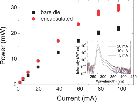
The use of encapsulation produced a 35%increase in light output power at 20mA CW injection current from 6.9mW to 9.3mW,"the highest power reported to date for DUV LED with emission shorter than 365 nm at this drive current".The encapsulated chip gave 30mW light output power at 100mA(Figure 1).The researchers attribute 9%of the improved light extraction over a conventional device to the change from p-GaN to p-AlGaN and they attribute nearly 30%of the improved light extraction to the encapsulation.
The peak emission occurred at 278nm,with a secondary peak around 320nm,probably related to recombination in the p-AlGaN.The parasitic peak needs to be reduced through prevention of spill-over of electrons into the p-contact by adding a suitable electron-blocking layer.
The EQE of the encapsulated device was 10.4%at 20mA,compared with 7.8%for the device without.A peak EQE for the encapsulated LED of 12%was attained at lower current.The wall-plug efficiency(WPE)of the encapsulated device was 5.5%at 20mA due to the high forward voltage of 8.4V.
The researchers see the development of DUV LEDs with wall-plug efficiencies greater than 10%as an enabling condition for their use in power-demanding applications,such as disinfection,decontamination,and curing.
The researchers comment:"Further optimization of the p-layer heterostructure and vertical conductivity is needed for the reduction of the forward voltage and higher WPE".
Devices with larger active areas of 0.5mm2(about 4x that of 350μm square device)reached peak EQEs of 10.9%at 20mA(a current density 4A/cm2)and WPEs of 7.8%.The researchers comment that their results indicate a significant reduction of non-radiative recombination associated with defects typically limiting efficiency at low current density.


