Singapore researchers have developed high-mobility III-V indium gallium arsenide (InGaAs) channel n-type metal-oxide-semiconductor field-effect transistors (n-MOSFET) on germanium-on-insulator (GeOI) substrates [Ivana et al, Appl. Phys. Express, vol5, p116502 2012].
The group, based at National University of Singapore (NUS) and Nanyang Technological University (NTU), comments: "To our best knowledge, this is the first demonstration of InGaAs surface channel n-MOSFET made on InGaAs-on-GeOI substrate."
So far, high-performance InGaAs devices have been grown on indium phosphide (InP) substrates. The aim for such devices is high performance at low power consumption at low cost. For mass production, InGaAs transistors need to be transferred to large-area silicon substrates – either by layer transfer from devices grown on InP (complex, expensive), or by direct growth on the substrate.
Previous InGaAs devices grown on silicon have been low performance due to low material quality resulting from poor lattice matching between silicon and III-V semiconductors. The lattice mismatch between InGaAs and Ge is smaller, and GeOI wafers have recently become commercially available. GeOI generally consists of a Ge layer on an insulating layer on silicon.
A further attraction of the GeOI approach is that Ge channels are a leading contender for the high-mobility p-MOSFETs that need to be combined with high-mobility n-MOSFETs to create complementary metal-oxide-semiconductor (CMOS) transistor circuitry.
Molecular beam epitaxy (MBE) was performed on GeOI with the (001) Ge surface offcut by 10° in the <111> direction. Offcut surfaces are used to overcome problems arising from the growth of polar III-V semiconductor on nonpolar Ge.
The Ge surface was prepared for MBE by annealing in vacuum at 650°C for 30 minutes. This treatment encouraged the formation of double atomic steps on the Ge surface. The MBE began with the deposition of about 10 monolayers of GaAs using migration-enhanced epitaxy (MEE) at 200°C.
"The double atomic steps, coupled with the MEE process, significantly suppress the formation of anti-phase domains at the III–V/Ge interface and the propagation of anti-phase boundary defects in the subsequent III–V layers grown on the Ge surface," the researchers explain. "Furthermore, the low growth temperature prevents interdiffusion between Ge and the III–V layers."
The epitaxial buffer structure was completed with a 500nm 580°C GaAs buffer, and a 1µm undoped metamorphic 420°C indium aluminium arsenide (InAlAs) buffer with indium composition graded between 0% and 52%. The 540°C InGaAs transistor channel layers grown on the relaxed InAlAs surface consisted of 15nm of beryllium-doped 70% In material on 35nm of more heavily doped 53%-indium semiconductor.
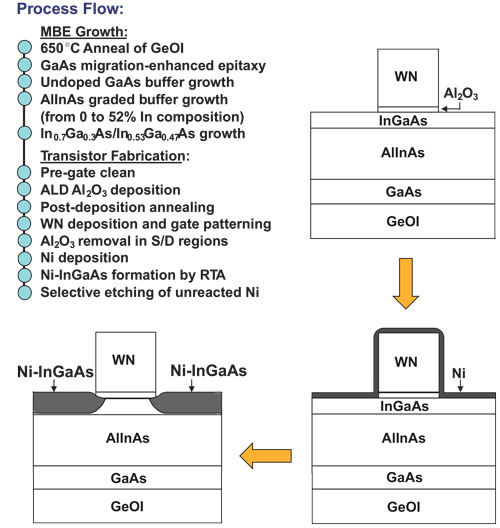
To make transistors (Figure 1), the epitaxial material was stripped of its native oxide and passivated in ammonium sulfide. The gate oxide of 8nm aluminium oxide (Al2O3) was applied using atomic layer deposition (ALD) and annealed at 400°C for a minute. The gate stack was capped with tungsten nitride (WN).

Figure 1: Process flow used, including growth of InGaAs on GeOI and fabrication of n-MOSFET. Schematics on right illustrate the self-aligned metallic S/D formation scheme that was employed.
The source-drain contacts were produced by etching down to the InGaAs and applying nickel through sputtering and rapid thermal annealing at 250°C for a minute. Unreacted nickel was removed using nitric acid solution.
Devices with gates 2µm long and 100µm wide were tested and found to have performance comparable with InGaAs transistors produced on InP substrates. At a drain bias of 1.2V, the on-state current was 203µA/µm with a gate overdrive of 2.5V (i.e. difference between gate potential and threshold). The peak extrinsic transconductance was 139µS/µm. Correcting for the parasitic resistance of the source-drain regions, the peak intrinsic transconductance was estimated to be ~227µS/µm.
The on/off ratio was two orders of magnitude (~102). This poor value was due to current leakage between the gate and drain, degrading performance. The researchers suggest that this could be due to incomplete removal of nickel at the end of the source-drain formation process.

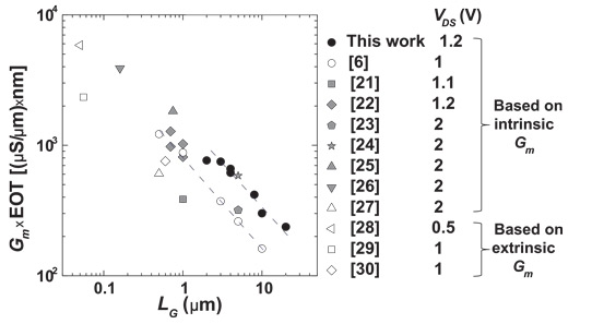
Figure 2: Normalized peak transconductance Gmxtox plotted as function of gate length (LG). Device performance obtained by NUS/NTU (black solid symbols) is compared with those reported in other InGaAs-channel n-MOSFETs in the literature (gray solid symbols for 70% In, open symbols for 53% In). The Gm data are from various drain biases, as shown (VDS). Gmxtox obtained in NUS/NTU work is significantly higher than those of In0.53Ga0.47As MOSFETs fabricated on silicon (open circles) [6]. Connecting dashed lines are intended only as a guide for the eye.
The researchers compared their peak intrinsic transconductance (normalized with respect to the equivalent oxide thickness of the gate dielectric: Gmxtox) with the values obtained by other groups with state-of-the-art InGaAs transistors (Figure 2). "Our data (black solid symbols) fits very well with other reported values on the inverse proportional trend of Gm versus LG," the researchers comment, adding: "Further reduction of the graded buffer layer could enable integration of III–V n-MOSFETs and Ge p-MOSFETs on a common platform."


